Copyright © 2021 TONG HSING

TONG HSING
Reality / Integrity / Customer First

TONG HSING
Reality / Integrity / Customer First

TONG HSING
Reality / Integrity / Customer First

TONG HSING
Reality / Integrity / Customer First

TONG HSING
Reality / Integrity / Customer First
- 1975
Corporation Founded
- 1979
Branched out into microelectronic element packaging
- 1994
Philippine subsidiary founded
- 1996
Branched out into wireless communication components
- 2007
Listed on the Taiwan Stock Exchange
- 45
years of experiences in technical product manufacturing
ABOUT
Stability, Integrity and Customers Satisfactions
TONG HSING ELECTRONIC IND., LTD. was established in 1974 in Yingge, New Taipei City, Taiwan. With its expertise in the development and production of thick film substrates and customized semiconductor micro-module packaging, TONG HSING is dedicated to research and development, process optimization and the provision of customer satisfaction.
TONG HSING's packaging services and substrate manufacturing technologies are now widely used in the applications of wireless communications, MEMS, image sensors, optoelectronic semiconductor components, LEDs, solar cells, automotive electronics, computer peripheral components, medical and networking equipment. In addition, TONG HSING ELECTRONIC IND., LTD. provides wafer probing, backgrinding, wafer reconstruction, assembly, automated inspection and finished module testing services for image sensor, MEMS and biomedical inspection products.。
READ MOREAPPLICATIONS產品應用

Wireless Communication

MEMS

Image Sensor
Optoelectronic Devices
LED

Solar Cells

Automotive Electronics

Computer Peripheral Components

Medical Electronics

Networking Equipment
PRODUCTS產品服務
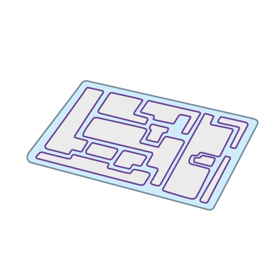
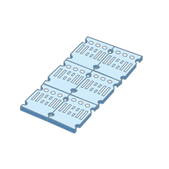
Power Semiconductors
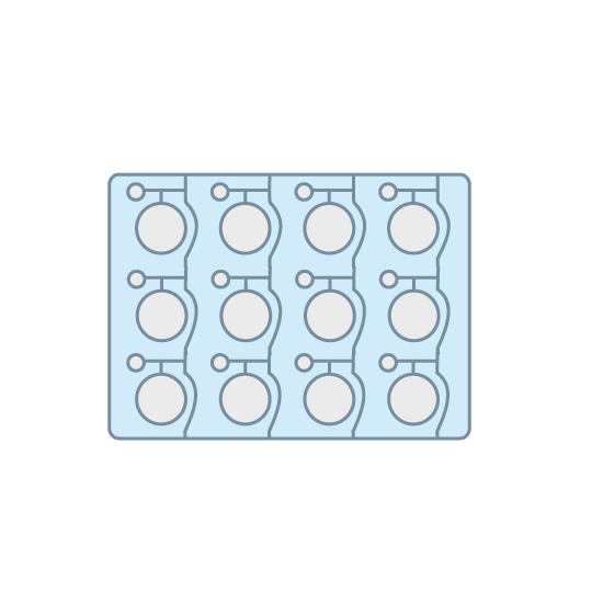
Direct Plated Copper
This process utilizes sputtering and photolithography processes to form circuit patterns on the ceramic substrates. By using the sputtering process, the bonding strength between the metal and the ceramic is extremely rigid; the traces and pads are not easy to lift-off. Moreover, the circuit pattern is more precisely positioned with high density of line width/spacing compared to the conventional thick film printing process.
This technique is mainly used in the fields of high brightness, high-power LED, RF microwave communication, laser system, and semiconductor equipments, etc.
Active Metal Brazing
Thick Film Printed Circuit Substrates
LATEST NEWS最新消息
READ MORE-
 12.Nov.2024
TongHsing Assists with LED lighting in rural, non-mountainous, and non-urban schools in New Taipei, Taoyuan, and Hsinchu.
-
 14.Feb.2023
Work together for local sustainability!
-
 16.Jan.2023
"Tong Hsing Electronics, Partnering to Extend Love"
-
 08.Jun.2022
Tong Hsing AGM elect the new Board member
-
 29.Nov.2021
6th Outstanding Enterprise Award Ceremony